

As a crucial tool for PCB through-hole copper inspection, the future development of the Hitachi CMI500 ETP probe will be influenced by industry technological advancements and changing market demands, exhibiting the following trends:
Improved Accuracy and Efficiency: With the evolution of PCBs towards High-Density Interconnect (HDI) boards and IC substrates, the demand for micron-level and even sub-micron-level defect detection is increasing. The Hitachi CMI500 ETP probe may further improve its detection accuracy. Currently, it boasts a detection accuracy of ±0.05μm. Future technological innovations, such as optimized electromagnetic coupling technology, may further enhance its accuracy and detection speed to meet the demands of high-end PCB production lines for rapid and precise inspection.
Integration of Intelligence and Automation:Artificial intelligence and big data technologies will be more deeply applied to probe inspection. The CMI500 ETP probe may integrate intelligent analysis functions in the future, automatically analyzing and processing inspection data. This will not only detect anomalies in through-hole copper thickness but also predict potential quality issues through data analysis, providing a more comprehensive quality control solution for PCB production. Simultaneously, its integration with production line automation systems will be higher, achieving seamless integration and improving the automation level of the entire production process.
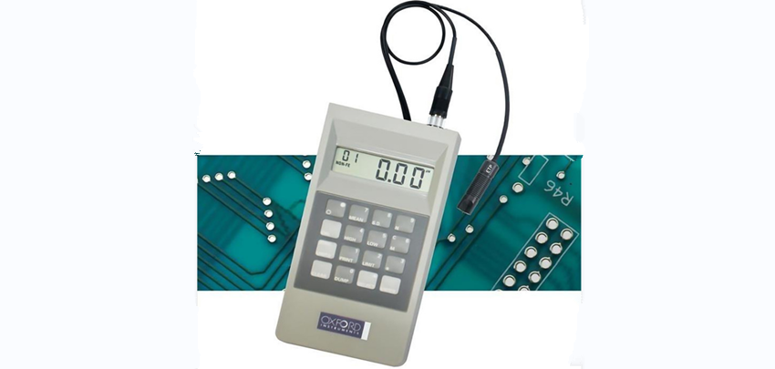
Multi-functional Integration: In the future, the CMI500 ETP probe may integrate more sensors or functional modules to detect other PCB parameters, such as plating composition analysis and hole wall roughness detection, becoming a comprehensive PCB inspection tool. This will provide PCB manufacturers with richer inspection information, helping them better control product quality.
Adaptability to Complex Environments and Materials: With the continuous innovation of PCB materials and the diversification of application environments, the CMI500 ETP probe needs to have better environmental adaptability and material compatibility. For example, for new conductive materials such as nanocrystalline copper, the probe needs to be able to accurately detect the thickness of the copper in the holes, while maintaining stable performance under more complex temperature and humidity conditions.
Miniaturization and Portability Improvements: Considering the inspection needs of different positions on the PCB production line and the convenience of on-site inspection, the CMI500 ETP probe may be further optimized in design while maintaining performance, achieving miniaturization and portability, making it convenient for operators to perform rapid inspections in different positions, and improving inspection efficiency and flexibility.